Saturday, October 28, 2017

I rather want you to try this App


MIFARE Classic Tool - MCT

This is an Android NFC-App for reading, writing, analyzing, etc. MIFARE® Classic RFID-Tags.


GENERAL INFORMATION
This tool provides several features to interact with (and only with) MIFARE Classic RFID-Tags.
It is designed for users who have at least basic familiarity with the MIFARE Classic technology.


┏━┫ PLEASE READ ┣━
┃Please read the whole page and make sure you got everything right before rating. Thank you!
┃If you rate with less then 4 stars, please leave a comment why. This way I can improve this app.
┃If you like MCT please consider to buy the donate version.
┗━


FEATURES
• Read MIFARE Classic tags
• Save and edit the tag data you read
• Write to MIFARE Classic tags (block-wise)
• Clone MIFARE Classic tags
(Write dump of a tag to another tag; write 'dump-wise')
• Key management based on dictionary-attack
(Write the keys you know in a file (dictionary). 
MCT will try to authenticate with these
keys against all sectors and read as much as possible.)
• Format a tag back to the factory/delivery state
• Write the manufacturer block of special MIFARE Classic tags
• Create, edit and save key files (dictionaries)
• Decode & Encode MIFARE Classic Value Blocks
• Decode & Encode MIFARE Classic Access Conditions
• Compare dumps (Diff Tool)
• Display generic tag information
• Display the tag data as highlighted hex
• Display the tag data as 7-Bit US-ASCII
• Display the MIFARE Classic Access Conditions as a table
• Display MIFARE Classic Value Blocks as integer
• In-App (offline) help and information
• It's open source (GPLv3) ;)


https://play.google.com/store/apps/details?id=de.syss.MifareClassicTool&hl=en

I previsouly checked if MILFARE RFID was based on hitag2 encryption. It is, 125 Khz...

to be more pratical, and to give some cash to friends here..I think this paper is much more important GONE IN 360 SECONDS HACK A HITAG2 ALGORITHM AND GET A BMW! OR A FERRARI! OR A PORCHE! WHATEVER..

Ok, hackers offer 1 million bitcoins for supposing hack a microchip (silicon)


Reverse engineering the ARM1 processor's microinstructions


This article looks at how the ARM1 processor executes instructions. Unexpectedly, the ARM1 uses microcode, executing multiple microinstructions for each instruction. This microcode is stored in the instruction decode PLA, shown below. RISC processors generally don't use microcode, so I was surprised to find microcode at the heart of the ARM1. Unlike most microcoded processors, the microcode in the ARM1 is only a small part of the control circuitry.

 should warn the reader in advance that this article is more terse than my usual articles and intended for the small group of people interested in very low-level details of the ARM1. For the average reader I'd recommend my article Reverse engineering the ARM1 instead.

The microinstructions

Each instruction in the ARM1 is broken down into 1 to 4 microinstructions. These microinstructions are stored in the instruction decode PLA (which acts as a ROM).[1] The ARM1's microcode is stored as 42 rows of 36-bit microinstructions. The 42 rows are split into 18 classes of instructions, each consisting of 1 to 4 microinstructions. (The microcode sequencer supports looping, allowing it to handle the bulk data transfer instructions LDM and STM which can take up to 17 cycles.)To explain the microinstruction format, I'll use the LDR instruction as an example. The LDR (Load Register) instruction accesses the memory address stored in a base register Rn plus a constant offset from the instruction and stores the result into a destination register Rd, also updating the base register. (This is similar to the C code: Rd = *Rn++;)[2] The ARM1 takes three cycles (i.e. three microinstructions) to perform this LDR operation. In the first cycle, the ALU adds the offset to the register to compute the address. The second cycle is used to fetch the word from memory. In the third cycle, the data is transferred to the destination register.
The diagram below shows the bit pattern for the LDR instruction. The PLA uses the highlighted bits (4, 20, 24-27) to determine the instruction class; the lighter bits are irrelevant for selecting the LDR instruction and are ignored. The cond bits specify a condition; if the condition is false, the instruction is skipped. The PUB, and W bits control different options for the LDR instruction. The Rn and Rd fields specify the base address register and the destination register. Finally, the 12-bit Offset field specifies the offset added to the base address.
Structure of the LDR (Load Register) instruction. Highlighted bits are used for instruction decoding; dark bits indicate LDR. Rn is the base register and Rd is the destination register.

Structure of the LDR (Load Register) instruction. Highlighted bits are used for instruction decoding; dark bits indicate LDR. Rn is the base register and Rd is the destination register.
Of the 32 instruction bits, only the 6 highlighted bits are used to select the microinstruction. As a result, microinstructions correspond to classes of instructions and the control outputs from the PLA are somewhat generic, e.g. "store to a register" rather than "store to register R12". Hardwired control logic looks at other bits in the instruction to pick a specific register, to pick a specific ALU operation, or to tweak exactly what the instruction does. For example, for LDR the microcode ignores the PUB and W bits and the hardwired control logic uses them. For registers, the microinstruction indicates which instruction bits specify the register and the hardwired register control logic uses those bits to select the register.

Contents of the microcode PLA

The raw data from the PLA for the LDR immediate instruction is given below, showing the 36 output bits forming a microinstruction for each cycle of the instruction.

Cycle numberPLA output
0001010101001000000100001100010100001
1101011010001000000001000111010100100
2010101101001000001010010110010010000
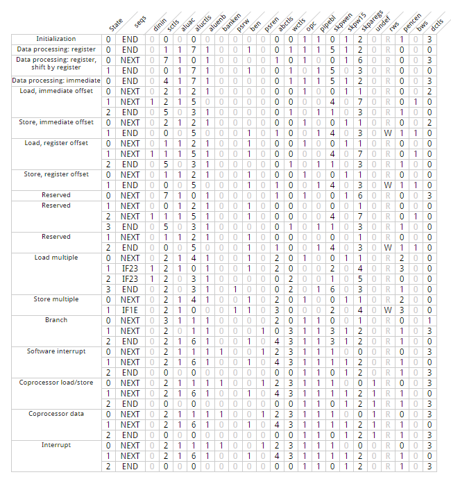
Since the raw PLA output is fairly meaningless, I have broken it down into fields and done a small amount of decoding. The image below shows the decoded contents of the instruction decode PLA; click for full-size. Each row corresponds to one clock cycle in an instruction and each column is one of the 22 fields generated by the 36 bits of the PLA. The PLA handles 18 different instruction groups, indicated on the left.
Contents of the ARM1 microcode PLA (thumbnail).

Contents of the ARM1 microcode PLA (thumbnail).
The rows Initialization and Interrupt are not instructions per se, but triggered by other PLA inputs. The Initialization micro-instruction is an idle step used when the pipeline does not have a valid instruction (at startup or after R15 modification). It is triggered if the iregval signal (8156) from the Pipeline State circuit is 0. The Interrupt microinstructions handle an interrupt or fault and are triggered by the intseq signal (8118) from the Trap Control circuit. The Reserved rows correspond to undocumented instructions, probably load and store with register-specified shift. The first Reserved row is unique in that the microcode sequence forks; this is cycle number 0 for both of the next Reservedblocks. It is unclear why these instructions were implemented but not documented.

Example microinstructions

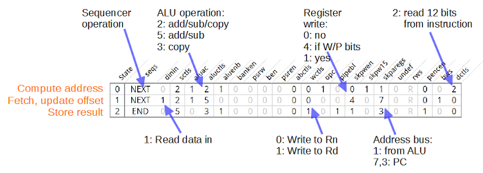
The diagram below illustrates the three microinstructions that make up the load register immediate (LDR) instruction, with explanations on some of the important fields. The first microinstruction computes the address: the indicated fields instruct the ALU to add or subtract the 12-bit offset value from the instruction, and put the value on the address bus. The ALU control logic uses the U (up/down) and P (pre/posts) bits in the instruction to determine if the offset should be added or subtracted or ignored. This illustrates that the microinstruction only partially defines the instruction; the hardcoded control logic also makes decisions based on the instruction. The microinstruction also specifies that the sequencer should move to the next microinstruction.The instruction decode PLA contents for the LDR (Load Register) immediate instruction. Each row corresponds to a clock cycles and shows the activity during one cycle. Each column indicates a control signal.

The instruction decode PLA contents for the LDR (Load Register) immediate instruction. Each row corresponds to a clock cycles and shows the activity during one cycle. Each column indicates a control signal.
The next microinstruction instructs the ALU to update the offset register. As before, the ALU control logic determines if the update requires an add or subtract. The register control logic determines if the register should be updated. The microinstruction also indicates that the fetched data should be read in.
The final microinstruction stores the fetched result in a register. It specifies Rd as the destination register and indicates a register write. The microinstruction tells the sequencer this is the end of the instruction.

Fields in the microinstruction

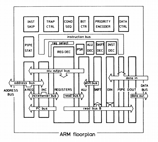
This section describes the fields that make up the microinstruction. I am still working out all the details, so this is not 100% accurate. Refer to the floorplan diagram below to see the components involved.Floorplan of the ARM1 chip, from ARM Evaluation System manual. (Bus labels are corrected from original.)

Floorplan of the ARM1 chip, from ARM Evaluation System manual. (Bus labels are corrected from original.)

seqs: sequencer control

This field specifies the cycle number for the next microinstruction. It is used by the Sequence Controller. It has the following values:
FieldLabelMeaning
0ENDEnd of the instruction
1NEXTMove to next cycle in sequence
2IF23If not pencz, next cycle is 2; if pencz, next cycle is 3.
3IF1EIf not pencz, next cycle is 1; if pencz, ends the instruction.
The pencz signal from the priority encoder indicates all registers have been processed for a LDM/STM instruction.
For more information, see Reverse engineering ARM1 instruction sequencing.
Signal numbers: 8310, 8309. I've put this field first to make control flow clearer, but it is physically after rws in the PLA.

dinin: data in to B bus

This field indicates the value on the data pins should be read in to the B bus. It is used by the data bus controls.Signal number: 8111

sctls: shifter controls

This field specifies the shifter action at a high level. The Shift Decode block uses this field in combination with other instruction bits and values to determine the specific shift direction and amount.
FieldShifter action
0Rs
1DP instruction
2ASL 2*instruction
3byte to word
4no shift
5ASL 2 bits
6nop (unused)
7nop
For more details, see Decoding barrel-shifter commands.
Signal numbers: 8288, 8287, 8286. Note that bits 2 and 1 are reversed coming out of the PLA.

aluac: ALU latch A bus

This signal latches the A bus value as an ALU input. The ALU control logic generates latch controls 2370, 2371 from this signal. For more details, see The ALU control logic.Signal number: 8058

aluctls: ALU mode controls

This field selects the ALU mode. The ALU decoder uses this field to generate the ALU control signals.
FieldOperationInstructions
0add/rsb for base register update / addressLDM/STM/Data processing
1add for branch/fault destinationB/SWI
2add/sub/nop for address computationLDR/STR
3mov for register update, nop for abortLDM/LDR
4add/rsb/mov for address computationLDM/STM
5add/sub for base register updateLDR/STR
6rsb for link address updateBL / SWI
7op specified by instructionData processing
For more details, see The ALU control logic.
Signal numbers: 8062, 8061, 8060

aluenb: ALU latch B bus

This signal latches the B bus value as an ALU input. The ALU control logic generates latch controls 7485, 7486 from this signal. For more details, see The ALU control logic.Signal number: 8063

banken: update PSR mode

This signal causes the M0, M1, F and I flags in the PSR to be updated from the psrbank signals from the trap control circuit. This happens during fault handling. This signal is used by the flag circuitry. For more details, see The ARM1 processor's flags.Signal number: 8075

psrw: PSR write

This signal indicates that the PSR is potentially being written by a LDM/STM block copy instruction. It controls writing the ALU bus to the flags, after some more logic. It also allows LDM/STM to access the user-mode registers via the S bit. This signal is used by the flag circuitry. For more details, see The ARM1 processor's flags.Signal number: 8273

nben: data to B bus

This signal indicates that the register file should write to the B bus when nben is 0. This signal is used by the register control logic and the flag logic. For more details, see The ARM1 processor's flags and Inside the ARMv1 Register Bank.Signal number: 8186; the signal is negative-active.

psren: PSR to B bus

When active, this signal enables writing the PSR to the B bus to save it during a trap. This signal is used by the flag logic. For more details, see The ARM1 processor's flags.Signal number: 8272

abctls: register controls for A and B bus

This field controls which registers are read onto the A and B bus. This signal is used by the register control logic.
FieldA register selectorB register selector
0Instruction bits 16-19 (Rn)Instruction bits 0-3 (Rm)
1Instruction bits 8-11 (Rs)Instruction bits 12-15 (Rd)
2R15Instruction bits 16-19 (Rn)
3R15From priority encoder
4Instruction bits 16-19 (Rn)R14
For more details, see Inside the ARMv1 Register Bank — register selection.
Signal numbers: 8042, 8041, 8040

wctls: register write controls

This field selects which register gets written to, from the ALU bus. This signal is used by the register control logic.
FieldRegister selector
0Instruction bits 16-19 (Rn)
1Instruction bits 12-15 (Rd)
2From priority encoder
3R14 (link)
For more details, see Inside the ARMv1 Register Bank — register selection.
Signal numbers: 8356, 8355

opc: OPC opcode fetch signal

This signal goes to the OPC pin and indicates a new instruction is being fetched. It is also used by the pipeline state circuitry.Signal number: 8630

pipebl: pipeline control

This signal is used by the pipeline state circuitry. It apparently indicates the end of the instruction, except for STM. It is high throughout branches and faults, perhaps to clear the pipeline.Signal number: 8261

skpwen: register write enable controls

This field controls whether a write to the register file happens or not. It is used by the Instruction Skip circuitry which can block the write if the instruction is aborted. The following table is a rough draft.
FieldWrite condition
0None
1Not dataabort
2Writeback
3Instruction bit 24 (link)
4Writeback / P bit
5alureg
6skpawen0
Signal numbers: 8324, 8323, 8322

skpw15: register 15 write controls

This signal controls writes to the R15 (PC). It is used by the Instruction Skip circuitry, perhaps to clear the pipeline when R15 is updated.Signal number: 8321

skparegs: address bus controls

This field controls what is written to the address bus. It is used by the Instruction Skip circuitry to generate the address bus controls. The following table is a rough draft.
FieldAddress source
0Trap address
1ALU bus
2incrementer (normal) or ALU bus (for R15 write)
3unincremented PC (normal) or ALU bus (for R15 write)
4ALU bus or PC or incrementer, depending on R15 write and priority encoder
5ALU bus or PC or incrementer, depending on R15 write and priority encoder
6incrementer
7unincremented PC (normal) or ALU bus (for R15 write)
For more details, see Inside the ARMv1 — the Read Bus B, ALU Output Bus, and Address Bus.
Signal numbers: 8320, 8319, 8318

undef: undefined instruction

This signal is generated for an undefined instruction (specifically a coprocessor instruction). It is used by the Trap Control circuitry to generate a fault.Signal number: 8348

rws: read or write select

This signal controls the RW output; it is 1 for a read and 0 for a write. The Trap Control circuitry gates this (apparently to block writes on an address exception) and the signal then drives the RW pin.Signal number: 8284

pencen: priority encoder A bus control

This field controls writing of the bit counter output (times 4) to the A bus. It can also set the two low bits, either for the constant 3, or to add 3 to the bit counter output. The constant 3 is used (with borrow) to subtract 4 from R14 during a branch with link, see page 233 of VLSI RISC Architecture and Organization. The modified bit counter output is used to compute the LDM/STM start address.
FieldBit counter action on A bus
0None
1Low bits set (3)
2Bit count
3Bit count, low bits set
Signal numbers: 8202, 8201

bws: enable byte/word select

This signal indicates that byte/word should be selected by instruction bit 22, for LDR/STR. This signal is used by the Data Control (field extraction) circuitry.For more details, see Inside the ARMv1 Read Bus.
Signal number: 8082

dctls: data bus field extraction controls

This field controls which bits of the data bus or instruction are passed to the B bus. This field is used by the Data Control (field extraction) circuitry.
FieldSelected data bus field
0Select a byte or word depending on bw
124 bits (branch offset)
212 bits (LDR/STR offset)
3byte (immediate instr)
For field 0, the byte is specified by controls 8195 and 8194.
For more details, see Inside the ARMv1 Read Bus or pages 296 and 301 of VLSI Risc Architecture and Organization.
Signal numbers: 8105, 8104

Microcode in RISC?

Everyone "knows" that RISC processors don't use microcode.[3] So does the ARM1 have "real microcode"?One of the ARM1 architects explains microcode: "A microcode address is formed from some or all of the contents of the instruction register, together with some state values which are internal to the micro-control unit. This address is decoded to drive a unique row of a matrix, the columns of which are the control signals for the datapath."[4] This description is a perfect fit for how the ARM1's control works, so it seems reasonable to consider the ARM1 to have microcode.
I think it's easiest to understand the ARM1's control logic by viewing it as microcode. However, there are couple reasons to consider it not "real microcode". One reason is that the ARM1 microcode is only a small part of the chip's control, as you can see in the die photo and floorplan earlier. The control signals are heavily modified by the instruction skip component and conditionals are handled by the conditional unit. This goes beyond vertical microcode, where logic expands the microcode's control signals; in the ARM1, this other circuitry can entirely override the control signals. In addition, the ARM1 uses separate circuitry (the priority encoder) to control the block data transfer instructions; the microcode just sits in a loop. (The ARM2 is similar with multiplication — a separate circuit controls multiplication.)
The ARM1's microcode is an order of magnitude smaller than other microcoded processors. The ARM1's microcode has a 42×36 microcode, for 1512 bits in total. The 8086 used a 504×21 microcode (over 10,000 bits) while the 68000 has a 544×17 microcode and 366×68 nanocode (over 34,000 bits).
Probably the biggest objection to calling the ARM1 microcoded is that the designers of the ARM chip didn't consider it that way.[4] Furber mentions that some commercial RISC processors use microcode, but doesn't apply that term to the ARM1. He describes ARM1's instruction decode as two-level structure. In the first level, the instruction decoder PLA differentiates instructions into classes with similar characteristics. The secondary decoding uses the information from the first level along with hardware to cope with all the possible operations. The first level is described as providing "broad hints" about which functions to choose, and the second level fills in the details with bits from the instruction.

Conclusion

So is the ARM1 microcoded or not? The instruction decoder is clearly made up of microinstructions executed sequentially or with branching. It makes sense to look at this as microcode. But on the other hand, the microcode is fairly simple and forms a small part of the total control circuitry. A large amount of hardcoded logic interprets the microinstruction outputs to generate the control signals. My conclusion is the ARM1 should be called "partially microcoded" or maybe "hybrid microcode / hardwired control".This article owes a lot to Dave Mugridge's analysis of the ARM1, especially Inside the ARMv1 — instruction decoding and sequencing. Thanks to the Visual 6502 team for the ARM1 simulator and data used in my analysis.

Notes and references

[1] While a typical PLA acts as structured logic gates generating signals (as in the Z-80 or 6502), the ARM1's PLA is different. Exactly one row is active at a time, so the PLA functions more like a ROM. There's a discussion of ROMs as PLAs in section 7.3.2.2 of The Architecture of Microprocessors.[2] My explanation of the LDR instruction is simplified, since the instruction provides a variety of addressing mechanisms. It also provides byte access as well as 32-bit word access. Full details are here.
[3] IBM's ROMP microprocessor is generally considered RISC, but uses a 256×34 control ROM. Likewise, the Intel i960 is usually considered RISC but uses microcode.
[4] ARM1 designer Furber's book VLSI RISC Architecture and Organization discusses the ARM1 and other RISC chips. Section 1.3.1 has an extensive discussion of microcode. He describes how the ARM1's block move and ARM2's multiplication operations are under the control of a separate hardware unit inside the chip, unlike how a microcoded implementation would operate. Section 4.7 describes the ARM1's control logic.


this tampering , also goes for RFID from ID


The visual presentation of the complete chromatogram showing all samples and standards side by side is one of the most convincing arguments for Thin-Layer Chromatography. No other chromatographic technique can directly express the result as a color image and make it available for visual evaluation.
To reproducibly acquire and preserve best quality images of TLC/HPTLC chromatograms under different illuminations this high-end imaging and documentation system is now available. With its new digital CCD camera a maximum resolution of 82 μm on the plate is obtained.
For electronic image acquisition the camera – like the human eye – captures polychromatic visible light. Under white light illumination it is the light reflected from the layer background. Under long-wavelength UV light (366 nm) it is the light emitted by fluorescent substances. When short-wavelength UV light (254 nm) is used, substances absorbing UV 254 appear as dark zones, provided the layer contains a fluorescence indicator (fluorescence quenching).

another technique for tampering microcontrollers Real time Data plot from serial port

Real time Data plot from serial port


It plots real time data from serial port. It can use for any serial port device.

%%real time data plot from a serial port 
% This matlab script is for ploting a graph by accessing serial port data in
% real time. Change the com values and all variable values accroding to
% your requirements. Dont forget to add terminator in to your serial device program.
% This script can be modified to be used on any platform by changing the
% serialPort variable. 
% Author: Moidu thavot.

%%Clear all variables

clear all;
%%Variables (Edit yourself)

SerialPort='com6'; %serial port
MaxDeviation = 3;%Maximum Allowable Change from one value to next 
TimeInterval=0.2;%time interval between each input.
loop=120;%count values
%%Set up the serial port object

s = serial(SerialPort)
fopen(s);


time =now;
voltage = 0;
%% Set up the figure 
figureHandle = figure('NumberTitle','off',...
    'Name','Voltage Characteristics',...
    'Color',[0 0 0],'Visible','off');

% Set axes
axesHandle = axes('Parent',figureHandle,...
    'YGrid','on',...
    'YColor',[0.9725 0.9725 0.9725],...
    'XGrid','on',...
    'XColor',[0.9725 0.9725 0.9725],...
    'Color',[0 0 0]);

hold on;

plotHandle = plot(axesHandle,time,voltage,'Marker','.','LineWidth',1,'Color',[0 1 0]);

xlim(axesHandle,[min(time) max(time+0.001)]);

% Create xlabel
xlabel('Time','FontWeight','bold','FontSize',14,'Color',[1 1 0]);

% Create ylabel
ylabel('Voltage in V','FontWeight','bold','FontSize',14,'Color',[1 1 0]);

% Create title
title('Real Time Data','FontSize',15,'Color',[1 1 0]);


%% Initializing variables

voltage(1)=0;
time(1)=0;
count = 2;
k=1;
while ~isequal(count,loop)
   
    %%Re creating Serial port before timeout
    
    k=k+1;  
    if k==25
        fclose(s);
delete(s);
clear s;        
s = serial('com6');
fopen(s)
k=0;
    end
    
    %%Serial data accessing 
    
     voltage(count) = fscanf(s,'%f');
     
     %%For reducing Error Use your own costant
     
     voltage(1)=0;     
     if (voltage(count)-voltage(count-1)>MaxDeviation)
         voltage(count)=voltage(count-1);
     end
     
     time(count) = count;
    set(plotHandle,'YData',voltage,'XData',time);
    set(figureHandle,'Visible','on');
    datetick('x','mm/DD HH:MM');
    
    pause(TimeInterval);
    count = count +1;
end


%% Clean up the serial port
fclose(s);
delete(s);
clear s;

https://www.mathworks.com/matlabcentral/fileexchange/28941-real-time-data-plot-from-serial-port?focused=5166995&tab=function

and about tampering, I have a gov contractor software to share

Data Visualizer
Oscilloscope


The oscilloscope module visualizes data values in real-time. It has four channels for monitoring four different data streams at the same time. Each channel's data stream is visualized as a graph in the plot area, each with a different color. The vertical position and amplitude of each channel can be modified. For repeating signals, or for capturing rare events, the oscilloscope has a trigger module. It also has cursors to measure various properties of the data streams.


Copy Protection in Modern Microcontrollers


This tamper resistance is not absolute: an opponent with access to semiconductor test equipment can retrieve key material from a chip by direct observation and manipulation of the chip's components. It is generally believed that, given sufficient investment, any chip-sized tamper resistant device can be penetrated in this way.


Non-Invasive attacks

The most widely used non-invasive attacks include playing around supply voltage and clock signal. Under-voltage and over-voltage attacks could be used to disable protection circuit or force processor to do wrong operation. For these reasons, some security processors have voltage detection circuit, but as a rule this circuit does not react to transients. So fast signals of various kinds may reset the protection without destroying the protected information.
Power and clock transients can also be used in some processors to affect the decoding and execution of individual instructions. Every transistor and its connection paths act like an RC element with a characteristic time delay; the maximum usable clock frequency of a processor is determined by the maximum delay among its elements. Similarly, every flip-flop has a characteristic time window (of a few picoseconds) during which it samples its input voltage and changes its output accordingly. This window can be anywhere inside the specified setup cycle of the flip-flop, but is quite fixed for an individual device at a given voltage and temperature. So if we apply a clock glitch (a clock pulse much shorter than normal) or a power glitch (a rapid transient in supply voltage), this will affect only some transistors in the chip. By varying the parameters, the CPU can be made to execute a number of completely different wrong instructions, sometimes including instructions that are not even supported by the microcode. Although we do not know in advance which glitch will cause which wrong instruction in which chip, it can be fairly simple to conduct a systematic search.
Another possible way of attack is current analysis. Using 10 - 15 ohm resistor in the power supply, we can measure with an analog/digital converter the fluctuations in the current consumed by the card. Preferably, the recording should be made with at least 12-bit resolution and the sampling frequency should be an integer multiple of the card clock frequency.
Drivers on the address and data bus often consist of up to a dozen parallel inverters per bit, each driving a large capacitive load. They cause a significant power-supply short circuit during any transition. Changing a single bus line from 0 to 1 or vice versa can contribute in the order of 0.5 - 1 mA to the total current at the right time after the clock edge, such that a 12-bit ADC is sufficient to estimate the number of bus bits that change at a time. SRAM write operations often generate the strongest signals. By averaging the current measurements of many repeated identical transactions, we can even identify smaller signals that are not transmitted over the bus. Signals such as carry bit states are of special interest, because many cryptographic key scheduling algorithms use shift operations that single out individual key bits in the carry flag. Even if the status-bit changes cannot be measured directly, they often cause changes in the instruction sequencer or microcode execution, which then cause a clear change in the power consumption.
The various instructions cause different levels of activity in the instruction decoder and arithmetic units and can often be quite clearly distinguished, such that parts of algorithms can be reconstructed. Various units of the processor have their switching transients at different times relative to the clock edges and can be separated in high-frequency measurements.
Other possible threat to secure devices is data remanence. This is the capability of volatile memory to retain information stored in it for some period of time after power was disconnected. Static RAM contained the same key for a long period of time could reveal it on next power on. Other possible way is to 'freeze' state of the memory cell by applying low temperature to the device. In this case static RAM could retain information for several minutes at -20ºC or even hours at lower temperature.

3. Invasive attacks

Despite to more complexity of invasive attacks some of them could be done without using expensive laboratory equipment. Low-budget attackers are likely to get a cheaper solution on the second-hand market for semiconductor test equipment. With patience and skill it should not be too difficult to assemble all the required tools for even under ten thousand US dollars by buying a second-hand microscope and using self-designed micropositioners. The laser is not essential for first results, because vibrations in the probing needle can also be used to break holes into passivation.
Invasive attacks start with the removal of the chip package. Plastic over the chip could be removed by knife. Epoxy resin around the chip could be removed using fuming nitric acid. Hot fuming nitric acid dissolves the package without affecting the chip. The procedure should preferably be carried out under very dry conditions, as the presence of water could corrode exposed aluminium interconnects. The chip is then washed with acetone in an ultrasonic bath, followed optionally by a short bath in deionized water and isopropanol. After that chip could be glued into a test package and bonded manually. Having enough experience it might be possible to remove epoxy without destroying bonding wires and smartcard contacts.
Once the chip is opened it is possible to perform probing or modifying attacks. The most important tool for invasive attacks is a microprobing workstation. Its major component is a special optical microscope with a working distance of at least 8 mm between the chip surface and the objective lens. On a stable platform around a socket for the test package, we install several micropositioners , which allow us to move a probe arm with submicrometer precision over a chip surface. On this arm, we install a probe needle. These elastic probe hairs allow us to establish electrical contact with on-chip bus lines without damaging them.
On the depackaged chip, the top-layer aluminium interconnect lines are still covered by a passivation layer (usually silicon oxide or nitride), which protects the chip from the environment and ion migration. On top of this, we might also find a polyimide layer that was not entirely removed by HNO3 but which can be dissolved with ethylendiamine. We have to remove the passivation layer before the probes can establish contact. The most convenient depassivation technique is the use of a laser cutter. The UV or green laser is mounted on the camera port of the microscope and fires laser pulses through the microscope onto rectangular areas of the chip with micrometer precision. Carefully dosed laser flashes remove patches of the passivation layer. The resulting hole in the passivation layer can be made so small that only a single bus line is exposed. This prevents accidental contacts with neighboring lines and the hole also stabilizes the position of the probe and makes it less sensitive to vibrations and temperature changes.
It is usually not practical to read the information stored on a security processor directly out of each single memory cell, except for ROM. The stored data has to be accessed via the memory bus where all data is available at a single location. Microprobing is used to observe the entire bus and record the values in memory as they are accessed.
It is difficult to observe all (usually over 20) data and address bus lines at the same time. Various techniques can be used to get around this problem. For instance we can repeat the same transaction many times and use only two to four probes to observe various subsets of the bus lines. As long as the processor performs the same sequence of memory accesses each time, we can combine the recorded bus subset signals into a complete bus trace. Overlapping bus lines in the various recordings help us to synchronize them before they are combined.
In order to read all memory cells without the help of the card software, we have to abuse a CPU component as an address counter to access all memory cells for us. The program counter is already incremented automatically during every instruction cycle and used to read the next address, which makes it perfectly suited to serve us as an address sequence generator. We only have to prevent the processor from executing jump, call, or return instructions, which would disturb the program counter in its normal read sequence. Tiny modifications of the instruction decoder or program counter circuit, which can easily be performed by opening the right metal interconnect with a laser, often have the desired effect.
Another approach to understand how particular microcontroller or smartcard work is to reverse engineer it. The first step is to create a map of a new processor. It could be done by using an optical microscope with a CCD camera to produce several meter large mosaics of high-resolution photographs of the chip surface. Basic architecture structures, such as data and address bus lines, can be identified quite quickly by studying connectivity patterns and by tracing metal lines that cross clearly visible module boundaries (ROM, RAM, EEPROM, ALU, instruction decoder, etc.). All processing modules are usually connected to the main bus via easily recognizable latches and bus drivers. The attacker obviously has to be well familiar with CMOS VLSI design techniques and microcontroller architectures, but the necessary knowledge is easily available from numerous textbooks.
Photographs of the chip surface show the top metal layer, which is not transparent and therefore obscures the view on many structures below. Unless the oxide layers have been planarized, lower layers can still be recognized through the height variations that they cause in the covering layers. Deeper layers can only be recognized in a second series of photographs after the metal layers have been stripped off, which could be achieved by submerging the chip for a few seconds in hydrofluoric acid (HF) in an ultrasonic bath. HF quickly dissolves the silicon oxide around the metal tracks and detaches them from the chip surface. HF is an extremely dangerous substance and safety precautions have to be followed carefully when handling it.
Where the implementation is familiar, there are a number of ways to extract information from the chip by targeting specific gates or fuses or by overwriting specific memory locations. Even where this is not possible, memory cells can be attacked; this can also be done on a relatively modest budget.
Most currently available microcontrollers and smartcard processors have feature sizes of 0.5 - 1 µm and only two metal layers. These can be reverse-engineered and observed with the manual and optical techniques described in the previous sections. For future chip generations with more metal layers and features below the wavelength of visible light, more expensive tools additionally might have to be used.
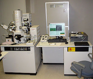
A focused ion beam (FIB) workstation consists of a vacuum chamber with a particle gun, comparable to a scanning electron microscope (SEM). Gallium ions are accelerated and focused from a liquid metal cathode with 30 kV into a beam of down to 5 - 10 nm diameter, with beam currents ranging from 1 pA to 10 nA. FIBs can image samples from secondary particles similar to a SEM with down to 5 nm resolution. By increasing the beam current, chip material can be removed with the same resolution. Better etch rates can be achieved by injecting a gas like iodine via a needle that is brought to within a few hundred micrometers from the beam target. Gas molecules settle down on the chip surface and react with removed material to form a volatile compound that can be pumped away and is not redeposited. Using this gas-assisted etch technique, holes that are up to 12 times deeper than wide can be created at arbitrary angles to get access to deep metal layers without damaging nearby structures. By injecting a platinum-based organometallic gas that is broken down on the chip surface by the ion beam, platinum can be deposited to establish new contacts. With other gas chemistries, even insulators can be deposited to establish surface contacts to deep metal without contacting any covering layers.
Using laser interferometer stages, a FIB operator can navigate blindly on a chip surface with 0.15 µm precision, even if the chip has been planarized and has no recognizable surface structures. Chips can also be polished from the back side down to a thickness of just a few tens of micrometers. Using laser interferometer navigation or infrared laser imaging, it is then possible to locate individual transistors and contact them through the silicon substrate by FIB editing a suitable hole. This rear-access technique has probably not yet been used by pirates so far, but the technique is about to become much more commonly available and therefore has to be taken into account by designers of new security chips. FIBs are used by attackers today primarily to simplify manual probing of deep metal and polysilicon lines. A hole is drilled to the signal line of interest, filled with platinum to bring the signal to the surface, where a several micrometer large probing pad or cross is created to allow easy access. Modern FIB workstations (for example the FIB 200xP from FEI) cost less than half a million US$ and are available in over hundred organizations. Processing time can be rented from numerous companies all over the world for a few hundred dollars per hour.

https://www.cl.cam.ac.uk/~sps32/mcu_lock.html

I surelly admit my humble knowldge of electronics...however if you want to decapp a microcontroller, try this approach instead of the microscope ion beams

125kHz RFID transceiver


The MLX90109 is a single chip RFID transceiver for the 125kHz frequency range. It has been conceived for minimum system cost and minimum power consumption offering all required flexibility for a state of the art AM transceiver base station.
An external coil (L) and capacitor (C) are connected as a parallel resonant circuit that determines the carrier frequency and the oscillator frequency of the reader. This eliminates zero modulation effects by perfect antenna tuning, and avoids the need for an external oscillator.
The reader IC can easily be switched to power down by setting the antenna amplitude to zero.
The MLX90109 can be configured to decode the transponder signal on-chip. In this case the decoded signal is available through a 2-wire interface with clock and data. For minimum interface wiring, the non-decoded transponder signal can also be made available on a single wire interface.

the russians the other day, we're saying to me...about the decapping the microchips...the contact with air destruction and everything or else...

Hacker extracts crypto key from TPM chip


An American hacker has, with a great deal of effort, managed to crack a Trusted Platform Module (TPM) by Infineon. He was able to read the data stored on the TPM chip, for instance cryptographic keys (RSA, DES) such as those also used by Microsoft's BitLocker on appropriate motherboards.
TPM hardware incorporates various levels of logical as well as physical measures designed to counter a range of attacks, such as differential electromagnetic analyses (DEMA) and even physical intrusions. Once the keys are retrieved, however, an attacker can read the encrypted data stored on a hard disk without needing a password.
Previously known as the smart card hacker, Christopher Tarnovsky of Flylogic Engineering has presented his work at the Black Hat DC security conference. He apparently managed to suss out a processor in the "SLE 66CLX360PE"PDF family used in the TPM. For this purpose, he extracted the actual chip from the housing in his special lab using various procedures that involved liquids and gases (a video about this is available online).
He then worked his way through the different layers of the chip using, for instance, a Focused Ion Beam microscope and Photoshop to figure out the chip's structure and find a way into the heart of the TPM. Subsequently, he analysed the on-chip signalling pathways to obtain access to the processor's data bus. This took Tarnovsky the better part of six months and numerous TPM chips. However, retrieving the license key of an XBox 360, which also contains Infineon's TPM, apparently only required an additional six hours.
While Tarnovsky says that Infineon has so far said such attacks just weren't feasible, Peter Laackmann, Infineon's Senior Principal for Chip Cards & Product Security, in an interview with The H's associates at heise Security, denied this is the case. The executive said that Infineon does not rule out the possibility of successful attacks. Laackmann said that TPM chips are not uncrackable and are not advertised as such. The potential for such an attack was already evident in an earlier evaluation phase and had apparently been carried out successfully by company researchers, quite some time ago. However, one mustn't neglect the effort involved in such an attack, said Laackmann, adding that even Tarnovsky himself admits that the necessary steps aren't easy to reproduce and require a considerable amount of special equipment. According to Tarnovsky, the required lab equipment represents an investment of about $200,000.
Laackmann also said that the product family has become obsolete, and that the cracked processor was only intended for smart cards. There is a new generation of TPM chips based on the SLE78 family, which apparently offers not only further physical anti-intrusion measures, but also additional cryptographic features. In these chips, recording data bus traffic after breaking into the housing is said to be ineffective because the data is encrypted. Infineon's Integrity Guard concept is designed to avoid the transmission and processing of plain text data altogether. However, so far, few devices incorporate these new chips.
The hack's potential consequences for the many TPM-protected systems in corporate environments, for instance, are difficult to predict. One can hardly assume that criminals will reproduce such attacks on a practical level in the medium term. However, intelligence agencies could use the technology in targeted attacks – perhaps they are doing so already. Tarnovsky does not intend to publish the details of his approach – but he is also a business man. He plans to test the security of other vendors' TPMs in the near future.

Hello world! About decrypting the elliptic curve at a London restaurant


Put simply, Smaart is an analyzer – A dual-channel, FFT-based software platform we use in our work as audio engineers to view the frequency content of signals or measure the response of our electrical and electro-acoustic systems. Much like medical instrumentation for doctors, this tool helps us examine our sound systems in detail and diagnose and solve problems. Because Smaart is a software product, it provides the power of extremely powerful hardware-based analyzers in a package that is affordable by an average audio professional.
As mix engineers, we use Smaart to identify tones/frequencies of interest and help us with tasks like feedback suppression and channel equalization. As system engineers, it assists us in the process of setting up and aligning our speaker systems in our performance environment.
The name Smaart was derived from System Measurement Acoustic Analysis Real-time Tool, but that bit of trivia has been mostly consigned to the island-of-obscure-acronyms.
System Measurement Acoustic Analysis Real-time Tool (SMAART):
System Measurement – This is a dual-channel analyzer.  We can look at individual channels and take those signals apart to examine their level, frequency content, duration, etc . . . and we can compare two signals, the “what went in” of a system to the “what came out,” to determine what happened in between. In other words, what our systems (electronics, speakers, acoustical environments) are doing to the signals passing through them (frequency response, impulse response.)
Acoustic Analysis –  By doing system measurements in and of acoustic environments (where cool things like shows happen), we can use those measurements to help figure out how we can adapt our sound systems to our rooms, or even vice versa.Eddie Mapp Evanesence Dubai
Real-time Tool – This extremely powerful analyzer was actually built to be used, not as an academic experiment, but when and where we actually use our sound equipment – real-time in our shops, at our install sites, during our load-ins, and most importantly, in our actual show environments